Semiconductor


- Materials that permit flow of electrons are called conductors (e.g., gold, silver, copper, etc.).
- Materials that block flow of electrons are called insulators (e.g., rubber, glass, Teflon, mica, etc.).
- Materials whose conductivity falls between those of conductors and insulators are called semiconductors.
- Semiconductors are “part-time” conductors whose conductivity can be controlled. Silicon is the most common material used to build semiconductor devices

Special points about Silicon
- Atoms in a pure silicon wafer contains four electrons in outer orbit (called valence electrons).
- Germanium is another semiconductor material with four valence electrons.
- In the crystalline lattice structure of Si, the valence electrons of every Si atom are locked up in covalent bonds with the valence electrons of four neighboring Si atoms.
- In pure form, Si wafer does not contain any free charge carriers.
- An applied voltage across pure Si wafer does not yield electron flow through the wafer.
- A pure Si wafer is said to act as an insulator.
- In order to make useful semiconductor devices, materials such as phosphorus (P) and boron (B) are added to Si to change Si’s conductivity.
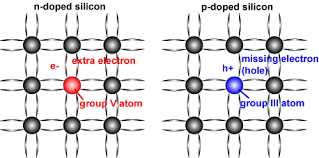
N-Type Silicon
- Pentavalent impurities such as phosphorus, arsenic, antimony, and bismuth have 5 valence electrons.
- When phosphorus impurity is added to Si, every phosphorus atom’s four valence electrons are locked up in covalent bond with valence electrons of four neighboring Si atoms. However, the 5th valence electron of phosphorus atom does not find a binding electron and thus remains free to float. When a voltage is applied across the silicon-phosphorus mixture, free electrons migrate toward the positive voltage end.
- When phosphorus is added to Si to yield the above effect, we say that Si is doped with phosphorus. The resulting mixture is called N-type silicon (N: negative charge carrier silicon).
- The pentavalent impurities are referred to as donor impurities.

P-Type Silicon
- Trivalent impurities e.g., boron, aluminum, indium, and gallium have 3 valence electrons.
- When boron is added to Si, every boron atom’s three valence electrons are locked up in covalent bond with valence electrons of three neighboring Si atoms. However, a vacant spot “hole” is created within the covalent bond between one boron atom and a neighboring Si atom. The holes are considered to be positive charge carriers.
- When a voltage is applied across the silicon-boron mixture, a hole moves toward the negative voltage end while a neighboring electron fills in its place.
- When boron is added to Si to yield the above effect, we say that Si is doped with boron. The resulting mixture is called P-type silicon (P: positive charge carrier silicon).
- The trivalent impurities are referred to as acceptor impurities.